The production of silicon discs, so-called wafers, with the highest quality standards is an essential part in the manufacturing chain of semiconductor devices. Proceeding from up to two metre long ingots, the semi-finished monocrystalline silicon product, individual wafers with a thickness of less than a millimetre are separated in a cutting operation. For example, the 200 mm wafers primarily utilised in IC (integrated circuit) applications have a thickness of ca. 880 pm after separating. For these cutting operations, multi-wire slicing (MWS) technology is the currently the most productive, state-of-the-art method.
Already during this segmentation into single wafers, fundamental wafer properties, elementary for subsequent manufacture, are determined. A precise and reliable cutting operation is exceedingly important, since every error committed here must — as much as is still possible — subsequently be eliminated by means of lapping, or alternatively with more modern grinding techniques, etching and finally polishing to improve the surface quality and wafer geometry. Only in this way can the extremely high requirements of chip manufacture be met. And only then can IC structures be applied by lithographic methods.
In the semiconductor industry, besides monocrystalline silicon, polycrystalline silicon is of the greatest importance, especially in the solar industry in the area of photovoltaic applications, and the second dominant area of application of MWS technology. In addition to these mass markets, MWS processes are also used, for example, in the manufacture of light-emitting diodes of the most varied materials such as silicon carbide (SiC), sapphire (Al2O3) and germanium (Ge). It is also employed in the manufacture of substrates made of innovative materials like gallium arsenide (GaAs) and other compound semiconductors. Conventional manufacturing technologies have limitations when cutting such materials, since there materials generally are characterised by high strength and brittleness.
Process Description
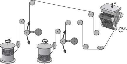
In multi-wire slicing technology (MWS), a cutting wire, proceeding from a coil, is guided over several deflection pulleys such that a field with parallel wire rows running in the same cutting direction is obtained (Fig. 9-9). Subsequently, the wire is wound up around a further coil. The wire is guided in a reversing fashion, whereby the amount of coiled wire of the respective cutting direction varies. For this reason, a partition of the wire field is constantly substituted with new and un
worn wire. The ingot to be cut is guided from above into the wire field. In this way several hundred wafers can be cut simultaneously in one cut.

The quality of MWS technology and that of alternative cutting processes is generally characterised by different factors. Besides the number of separable wafers per time unit, cut losses (due to the high material costs), surface roughness, wafer geometry and also the crystal damage depth of the wafers, designated as sub-surface damage (SSD), are especially relevant.
With respect to wafer geometry, the parameters of wafer thickness, wafer thickness fluctuation within a wafer (total thickness variation TTV) and bending of the wafer caused by procedural inaccuracies and internal stresses, so-called bows or warps, are very important and hence narrowly tolerated. Thus, for many applications, wafers are frequently needed that have a TTV of less than 20 qm after sawing.
The MWS method offers a number of advantages. Because of the simultaneous cutting of several hundred wafers, despite the low feed velocities of ca. 0.5 to 1 mm/min, productivity is increased by more than 400 % in comparison to inner diameter slicing (ID slicing) depending on the width of the wire field utilised. By using thin cutting wires with diameters smaller than 175 qm, cutting losses can be significantly reduced in comparison to other cutting technologies. The slight subsurface damage predestines these process kinematics especially to cutting very thin wafers. For applications in the area of photovoltaics, wafers of ca. 300 qm thickness have been state of the art for quite some time.
The trend towards larger wafer dimensions is also fulfilled by this method. The currently largest wafer diameter used in the semiconductor industry is about 300 mm, the edge length of the largest polycrystalline blocks used in the solar in
dustry amount to 150 mm. Cuts with these dimensions can be executed with modern MWS units [KAO99].
The process is subdivided with respect to the machining principle into two variants, the conventional and widely used cutting wire lapping and the newer cutting wire grinding. In the case of cutting wire grinding, the abrasive material is fixed on the tool with a bond system. As opposed to this, in lapping operations uncoated tools are used. Machining is made possible by supplying a lapping suspension, so-called slurry. The latter consists of a medium and an abrasive material.